- 您现在的位置:买卖IC网 > Sheet目录3879 > DSPIC30F6013T-20I/PF (Microchip Technology)IC DSPIC MCU/DSP 132K 80TQFP
2006 Microchip Technology Inc.
DS70117F-page 135
dsPIC30F6011/6012/6013/6014
19.0
12-BIT ANALOG-TO-DIGITAL
CONVERTER (A/D) MODULE
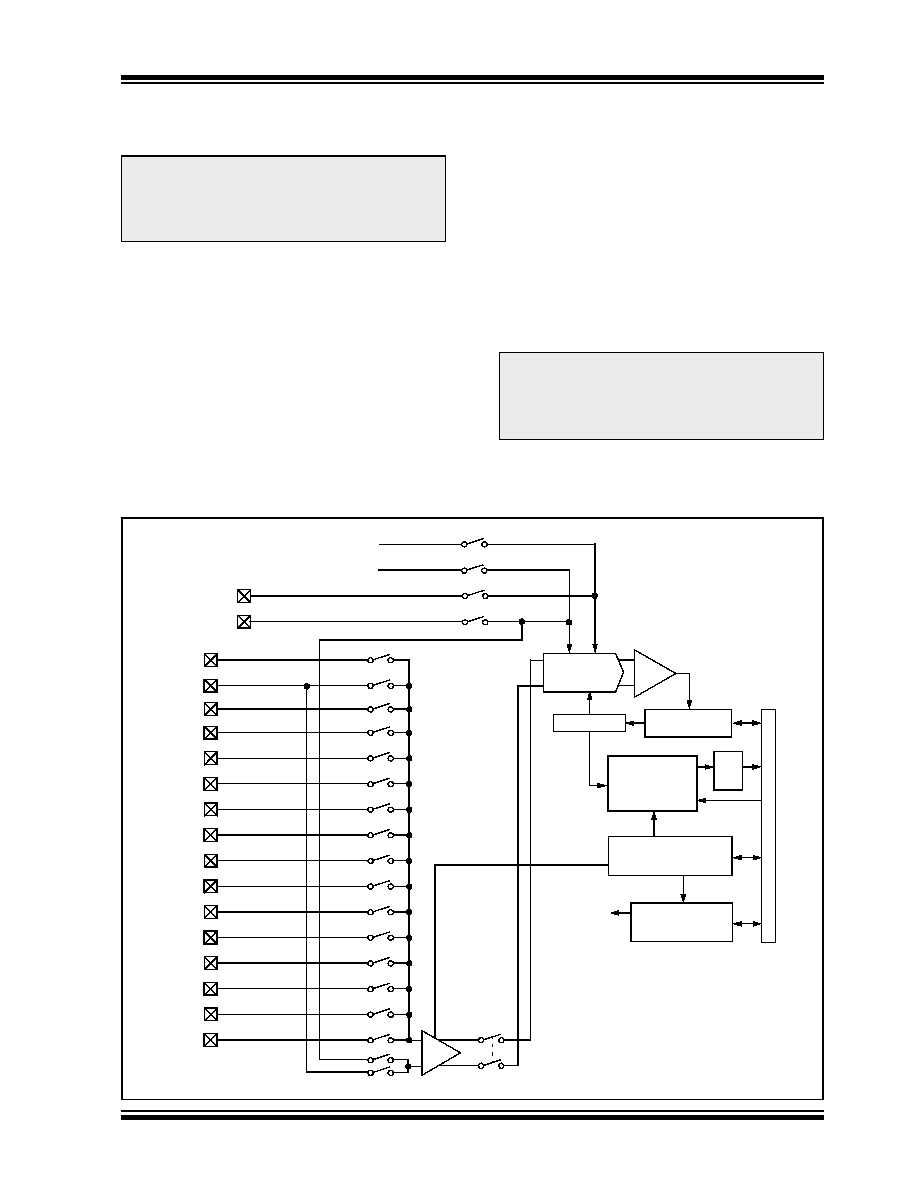
The 12-bit Analog-to-Digital Converter (ADC) allows
conversion of an analog input signal to a 12-bit digital
number. This module is based on a Successive
Approximation Register (SAR) architecture and pro-
vides a maximum sampling rate of 200 ksps. The ADC
module has up to 16 analog inputs which are multi-
plexed into a sample and hold amplifier. The output of
the sample and hold is the input into the converter
which generates the result. The analog reference volt-
age is software selectable to either the device supply
voltage (AVDD/AVSS) or the voltage level on the
(VREF+/VREF-) pin. The ADC has a unique feature of
being able to operate while the device is in Sleep mode
with RC oscillator selection.
The ADC module has six 16-bit registers:
ADC Control Register 1 (ADCON1)
ADC Control Register 2 (ADCON2)
ADC Control Register 3 (ADCON3)
ADC Input Select Register (ADCHS)
ADC Port Configuration Register (ADPCFG)
ADC Input Scan Selection Register (ADCSSL)
The ADCON1, ADCON2 and ADCON3 registers con-
trol the operation of the A/D module. The ADCHS reg-
ister selects the input channels to be converted. The
ADPCFG register configures the port pins as analog
inputs or as digital I/O. The ADCSSL register selects
inputs for scanning.
The block diagram of the 12-bit ADC module is shown
in Figure 19-1.
FIGURE 19-1:
12-BIT ADC FUNCTIONAL BLOCK DIAGRAM
Note: This data sheet summarizes features of this group
of dsPIC30F devices and is not intended to be a complete
reference source. For more information on the CPU,
peripherals, register descriptions and general device
functionality, refer to the “dsPIC30F Family Reference
Manual” (DS70046).
Note:
The SSRC<2:0>, ASAM, SMPI<3:0>,
BUFM and ALTS bits, as well as the
ADCON3 and ADCSSL registers, must
not be written to while ADON = 1. This
would lead to indeterminate results.
Comparator
12-bit SAR
Conversion Logic
VREF+
DAC
Dat
a
16-word, 12-bit
Dual Port
RAM
B
u
s
Inte
rf
a
c
e
AN12
0000
0101
0111
1001
1101
1110
1111
1100
0001
0010
0011
0100
0110
1000
1010
1011
AN13
AN14
AN15
AN8
AN9
AN10
AN11
AN4
AN5
AN6
AN7
AN0
AN1
AN2
AN3
CH0
AN1
VREF-
Sample/Sequence
Control
Sample
Input MUX
Control
Input
Switches
S/H
AVSS
AVDD
Fo
rm
a
t
发布紧急采购,3分钟左右您将得到回复。
相关PDF资料
DSPIC30F6012T-30I/PF
IC DSPIC MCU/DSP 144K 64TQFP
DSPIC30F6012T-20I/PF
IC DSPIC MCU/DSP 144K 64TQFP
DSPIC30F6011T-30I/PF
IC DSPIC MCU/DSP 132K 64TQFP
DSPIC30F6011T-20I/PF
IC DSPIC MCU/DSP 132K 64TQFP
DSPIC30F6010T-30I/PF
IC DSPIC MCU/DSP 144K 80TQFP
DSPIC30F6010T-20I/PF
IC PSPIC MCU/DSP 144K 80TQFP
PIC16C56A-20/P
IC MCU OTP 1KX12 18DIP
PIC16C621A-04I/P
IC MCU OTP 1KX14 COMP 18DIP
相关代理商/技术参数
DSPIC30F6013T-30I/PF
功能描述:数字信号处理器和控制器 - DSP, DSC 30MHz 132KB Flash RoHS:否 制造商:Microchip Technology 核心:dsPIC 数据总线宽度:16 bit 程序存储器大小:16 KB 数据 RAM 大小:2 KB 最大时钟频率:40 MHz 可编程输入/输出端数量:35 定时器数量:3 设备每秒兆指令数:50 MIPs 工作电源电压:3.3 V 最大工作温度:+ 85 C 封装 / 箱体:TQFP-44 安装风格:SMD/SMT
DSPIC30F6014-20E/PF
功能描述:数字信号处理器和控制器 - DSP, DSC 30MHz 132KB Flash RoHS:否 制造商:Microchip Technology 核心:dsPIC 数据总线宽度:16 bit 程序存储器大小:16 KB 数据 RAM 大小:2 KB 最大时钟频率:40 MHz 可编程输入/输出端数量:35 定时器数量:3 设备每秒兆指令数:50 MIPs 工作电源电压:3.3 V 最大工作温度:+ 85 C 封装 / 箱体:TQFP-44 安装风格:SMD/SMT
DSPIC30F6014-20I/P
制造商:Microchip Technology Inc 功能描述:MCU - Rail/Tube
DSPIC30F6014-20I/PF
功能描述:数字信号处理器和控制器 - DSP, DSC 20MHz 144KB Flash RoHS:否 制造商:Microchip Technology 核心:dsPIC 数据总线宽度:16 bit 程序存储器大小:16 KB 数据 RAM 大小:2 KB 最大时钟频率:40 MHz 可编程输入/输出端数量:35 定时器数量:3 设备每秒兆指令数:50 MIPs 工作电源电压:3.3 V 最大工作温度:+ 85 C 封装 / 箱体:TQFP-44 安装风格:SMD/SMT
DSPIC30F6014-20I/PF
制造商:Microchip Technology Inc 功能描述:16BIT 20MIPS DSPIC SMD 30F6014
DSPIC30F6014-30I/PF
功能描述:数字信号处理器和控制器 - DSP, DSC 30MHz 144KB Flash RoHS:否 制造商:Microchip Technology 核心:dsPIC 数据总线宽度:16 bit 程序存储器大小:16 KB 数据 RAM 大小:2 KB 最大时钟频率:40 MHz 可编程输入/输出端数量:35 定时器数量:3 设备每秒兆指令数:50 MIPs 工作电源电压:3.3 V 最大工作温度:+ 85 C 封装 / 箱体:TQFP-44 安装风格:SMD/SMT
DSPIC30F6014-30I/PF
制造商:Microchip Technology Inc 功能描述:16BIT 30MIPS DSPIC SMD 30F6014
dsPIC30F6014A-20E/PF
功能描述:数字信号处理器和控制器 - DSP, DSC 20MIPS 144 KB RoHS:否 制造商:Microchip Technology 核心:dsPIC 数据总线宽度:16 bit 程序存储器大小:16 KB 数据 RAM 大小:2 KB 最大时钟频率:40 MHz 可编程输入/输出端数量:35 定时器数量:3 设备每秒兆指令数:50 MIPs 工作电源电压:3.3 V 最大工作温度:+ 85 C 封装 / 箱体:TQFP-44 安装风格:SMD/SMT